
Improving the Design of Monolithically Integrated Magneto-Optic Routers
Whileelectro-optic(EO) routers are currently used in on-chip optical communication systems, they may require too much power for some applications. In these situations, we can look to monolithically integratedmagneto-optic(MO) routers as low-power alternatives. Designing these routers can be challenging. With multiphysics simulation, we can analyze on-chip MO routers and the manufacturing techniques used to create them.
Taking a Closer Look at Magneto-Optic Routers
Modern optical communication systems commonly use EO routers and macroscale MO devices. Each device, however, has its own drawbacks. EO routers require an electric field and often have operation voltages in the kilovolt range, while macroscale MO devices don’t allow for scalable solutions. The quest for small, low-power optic routing alternatives is thus an important focus for specialized researchers within this field. This search is complicated, as various specializations within physics and engineering are required to address the study and interaction of magnetism, magnetic materials, and light.
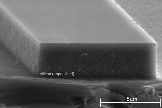
Scanning electron micrograph of an unpolished silicon-on-insulator rib waveguide used for optical routers on a chip. Image credit: J. Tioh, “Interferometric switches for transparent networks: development and integration,” 2012, Graduate Theses and Dissertations. Paper 12487.
One potential solution involves integrating optical components onto a silicon substrate to create an MO routing solution on a chip. This option reduces both the size and operation power of the device and can potentially enable new technologies like light processors. But before monolithically integrated MO routers become commonplace, there are still a few hurdles that this technology needs to overcome.
Standard industry practices, for instance, present a challenge when it comes to manufacturing monolithically integrated MO routers. To introduce new technology with minimal industry disruptions, standard practices must be used. In this case, silicon should be used as a base substrate and the combining materials must be compatible with silicon for successful monolithic integration. But bonding silicon and the suitable magneto-optic materials can be quite difficult using standard industry practices due to their crystal structures. As a result, the materials tend to become brittle and crack, significantly increasing optical losses.
Multiphysics simulation offers potential solutions to such challenges. These tools can help the research community identify optimal designs and manufacturing techniques for monolithically integrated MO routers. For his doctoral dissertation at Iowa State University, John Pritchard, an engineer who works within this field, turned to the COMSOL Multiphysics® software to provide new insight into the design and future of on-chip MO routers.
Analyzing the Components of an On-Chip MO System with COMSOL Multiphysics®
When analyzing an on-chip MO system, Pritchard chose to focus on a few key design elements. One point of focus was analyzing acodirectional coupler, a device that is commonly found in interferometer designs. The power coupling coefficients of a codirectional coupler vary based on the distance between the coupling section length and coupled waveguides. Through his simulation work, Pritchard determined how to generate an ideal power coupler coefficient by choosing a specific coupler length.
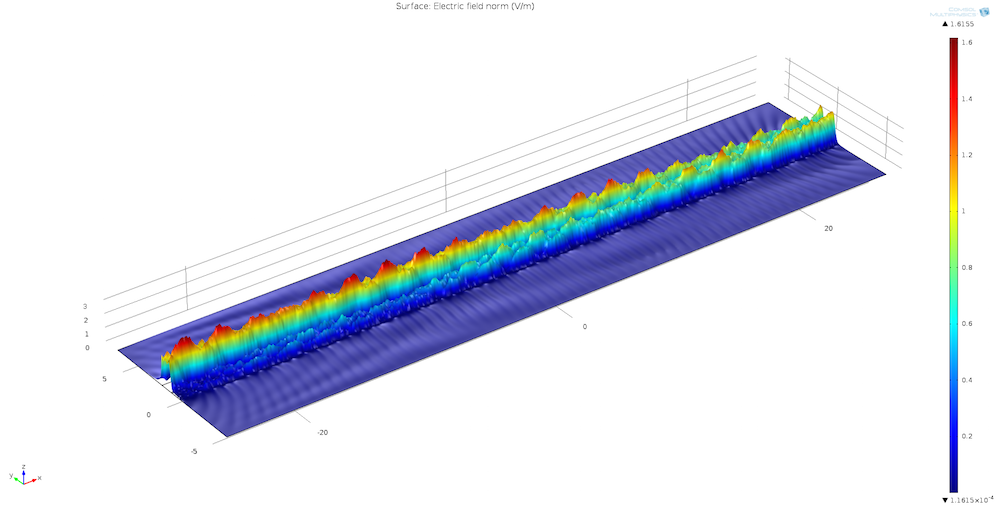
3D simulation results for the codirectional coupler. Copyright © John Pritchard.
Another point of analysis was anon-chip optical waveguide. The goal here was to design a rib waveguide that minimizes energy loss and maintains a sufficient beam profile throughout the device. To achieve this, Pritchard used silicon as the rib waveguide’s transmission medium, since it is suitably transparent to infrared light and useful for integration with electronic devices. Further, a low-index cladding model was placed between the substrate and waveguide to stop the optical mode from leaking out.
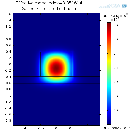
The optical mode of an SOI rib waveguide. Copyright © John Pritchard.
As for the waveguide’s silicon-on-insulator (SOI) platform, Pritchard used a buried oxide insulator on a silicon substrate. This waveguide configuration enabled him to confine relatively large optical modes in the waveguide and avoid harming the single-mode operation. Subsequent simulations of the configuration revealed that the optical mode is well confined within the waveguide and that this geometry can be used to design an interferometer. Pritchard also performed a frequency analysis of the top view of the design, as seen in the animation below and to the left. This waveguide design was deemed a success and is a significant step toward fully realizing MO routers on a chip.
Left: Wave propagation at the top of a dual waveguide and coupler at 1550 nm. Right: Mode profile of a coupler and dual waveguide. Copyright © John Pritchard.
Investigating the Effect of MO Material and the Design of a Magnetic Field Generator
The coupler and waveguide designs we’ve discussed thus far are ideal for the single-mode confinement of light at 1550 nm. Now, let’s see how adding a top layer of MO material to the SOI rib waveguide affects the device. Specifically, the goal is to find out the amount of light that is exposed to the Faraday rotation. This indicates when light with a rotated state of polarization interferes with nonrotated light.
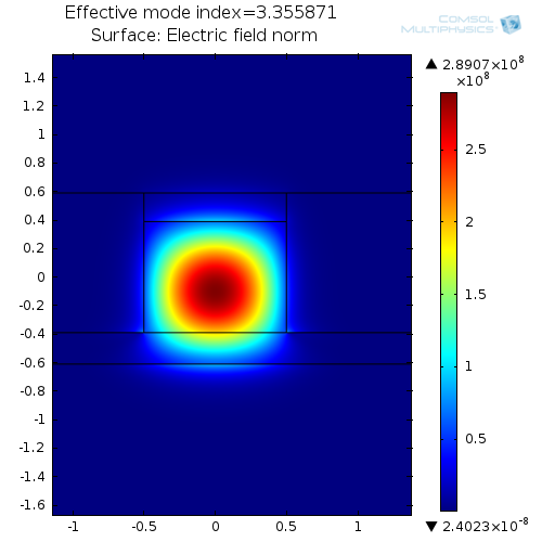
Mode analysis of an SOI waveguide with a top layer of MO material. Copyright © John Pritchard.
The results, highlighted above, show that the MO material contains 3.9% of the light. Despite being a small percentage, previous research suggests that this creates sufficient Faraday rotation to observe interference at the electrical output. But for this to happen, the material needs to be magnetized with a permanent magnet or controlled magnetic field generator. Finding appropriate monolithically integrated magnetic field generators was therefore a final point of consideration.
While magnetic field generation techniques are important for creating on-chip MO modulators, the process itself is complex. The small size of MO systems makes it difficult to develop monolithically integrated magnetic field generators. To address this, Pritchard used simulation to validate the design of a novel dynamic magnetic field generator: a four-turn integrated coil.

Left: Geometry of an integrated magnetic field generator. Right: Geometry of the integrated magnetic field generator with the MO material highlighted in pink and the silicon waveguide shown in purple. Copyright © John Pritchard.
The results show that the coil generated 260 G near the center of the optical waveguide when energized with a 35 mA current. Within the tested waveguide dimensions, this magnetic field strength can magnetize Ce:YIG film on silicon.
It is possible to expand such research by investigating the field at the center of the MO material, which is part of the core of the four-turn integrated coil. Here, the simulation studies indicate that with a current of 35 mA, the magnetic field at the center of the MO material layer has a maximum field of about 210 G, a reduction possibly explained by the difference in properties of the material. Such findings speak to the potential of on-chip MO routing solutions and can be used as a resource in improving their design and manufacturing processes.
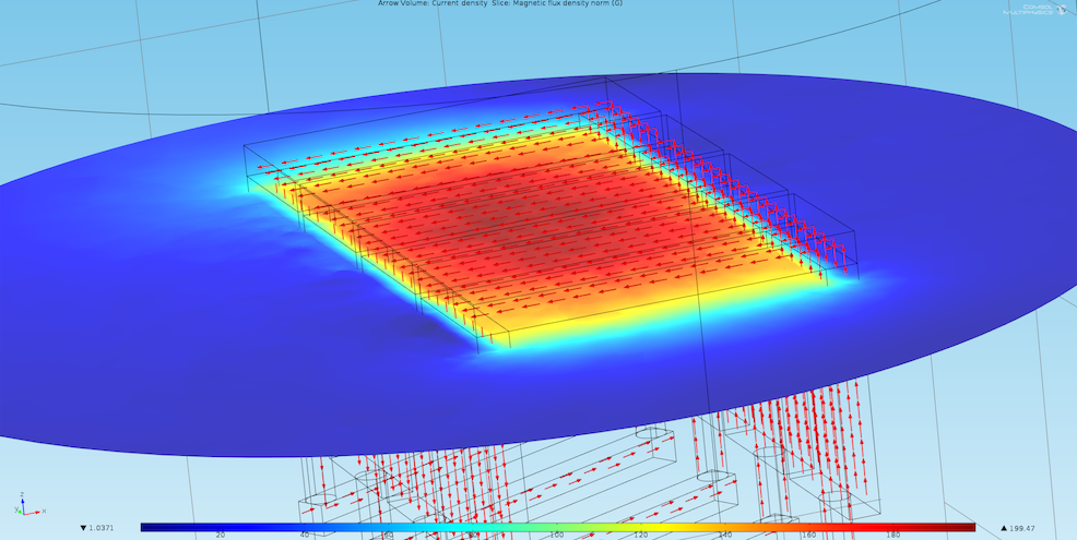
Simulation results for the magnetic field generator at the center of the coil. Copyright © John Pritchard.
Simulation Sheds Light on the Future of Optical Research
Future on-chip optical network architects will have a variety of active switching and routing options, allowing them to make their networks more robust by using both EO and MO devices. While it’s important to note that the results mentioned here are preliminary and more research is needed, the simulations and design methodologies act as a proof of concept for on-chip magnetic field generators and silicon rib waveguides. They can serve as a useful foundation for continued studies on such devices, creating a path for furthering their optimization.
As John Pritchard notes: “Some of the most beautiful connections between light, magnetism, and quantum theory have led to breathtaking technologies ranging from superconductor imaging to gigawatt laser pulses. These have enabled revolutionary inventions in transportation; measurement instruments used to understand the birth of the universe; and, in the near future, optical integrated circuits.” Looking to the future, we are eager to see the continued role of multiphysics simulation in advancing optical research, a field with wide-reaching applications.
Read More About Wave Optics Modeling
- Read the article that inspired this blog post inMagnetics Technology International2016: “Magneto-optic router on a chip”
- Browse theWave Optics categoryon the COMSOL Blog


Comments (2)
Rui Ma
October 16, 2018Hi. I am a beginner in Comsol. I also want to do simulation works about MO materials. Could you be so kind to share the tutorial model?
Brianne Costa
October 16, 2018 COMSOL EmployeeHello Rui,
Thanks for your comment.
For questions related to your modeling, please contact our Support team.
Online Support Center:https://www.comsol.com/support
Email:support@comsol.com