技术资料
白皮书和应用说明
Simple Finite Element Model of the Topografiner
发布日期2014
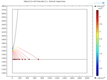
In our recent experiments we are revisiting the topografiner technology for the imaging of surface topography with a resolution of a few nanometers. In these new technique called Near-Field Emission Scanning Electron Microscopy (NFESEM), low-energy electrons are emitted from a polycrystalline tungsten tip via electric-field assisted tunneling. In order to characterize and improve the capabilities of our microscopes, in particular the vertical and lateral resolutions, we simulate the tunnel junction consisting of a metallic tip placed at distance d from a planar electrode and consider current versus voltage (I-V) and voltage versus distance (V-d) measurements.

下载
- cabrera_poster.pdf- 0.45MB
- cabrera_paper.pdf- 0.52MB
- cabrera_abstract.pdf- 0.46MB
