Improving High Voltage Stability of Vacuum Components with Comsol Shape Optimization
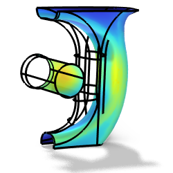
High voltage (HV) stability is an important requirement in many technical areas. The prevention of partial discharges or flashovers requires careful mechanical and electrical design of all components with high electric potential difference towards the surrounding. In the Semiconductor industry many machines, like electron beam lithography tools or scanning electron microscopes, rely on this stability. We deploy COMSOL Multiphysics at IMS Nanofabrication to enhance the research and development output by accelerating design processes. Design rules do exist for simple electrical conductive geometries, but complex 2D and 3D geometries need verification with e.g. finite element methods (FEM) in order to keep geometric field enhancement and therefore electric fields below a certain maximum value. For safety reasons, the maximum electric field is chosen e.g. more than a factor of two lower than the theoretical limit of 20kV/mm [1]. Using multiple cycles of mechanical design and verification are time consuming, but by utilizing the Comsol shape optimizer, this process is accelerated considerably. A draft 2D or 3D CAD geometry is imported and adapted to FEM needs with the design module. For large models, submodelling is prepared by doing a first coarse electrostatic (es) calculation. Subsequent geometry cutout and appropriate boundary settings then allow for the shape optimization step. The required objective function considers maximum electric fields at multiple sites, this is implemented by a pNorm for numeric stability. The resultant geometries can be exported to STL format for further processing with CAD software. Fig 1 shows the cutout results of a shape optimization for an axisymmetric electrode configuration. Several kV potential difference is applied between the upper and the lower electrode. For initial geometry and voltage settings (left plot), a maximum electric field norm of 7.3 kV/mm occurs at the lower electrode. While the shape of the lower electrode is fixed, the shape optimizer shifts the adjacent surface by max 0.54 mm, which reduces the max field at the lower electrode by over 10%, down to 6.4 kV/mm (right plot). Fig 2 depicts the results of a shape optimization at a 3D high voltage geometry. A cylindrical rod is placed close to a post like structure, with a voltage difference of several tens of kilovolts applied. The left plot shows the surfaces where the objective function is evaluated. The initial analysis, shown in the middle plot, yields high electric fields at several surfaces with small curvature. While geometry and position of the rod are fixed, a shape optimization of the post shifts and bends the posts away from the rod by max 1.1 mm, see plot on the right. This reduces the overall maximum field from 9.0 kV/mm by over 20%, down to 7.0 kV/mm.

下载
- eder-kapl_10852_poster.pdf- 1.91MB
